- 您现在的位置:买卖IC网 > Sheet目录3887 > PIC16F872T-E/SO (Microchip Technology)IC MCU CMOS 20MHZ 2K FLSH 28SOIC
103
8048C–AVR–02/12
ATtiny43U
output to the opposite clock edge of the data input sampling. The serial input is always sampled
from the Data Input (DI) pin independent of the configuration.
The 4-bit counter can be both read and written via the data bus, and it can generate an overflow
interrupt. Both the USI Data Register and the counter are clocked simultaneously by the same
clock source. This allows the counter to count the number of bits received or transmitted and
generate an interrupt when the transfer is complete. Note that when an external clock source is
selected the counter counts both clock edges. This means the counter registers the number of
clock edges and not the number of data bits. The clock can be selected from three different
sources: The USCK pin, Timer/Counter0 Compare Match or from software.
The two-wire clock control unit can be configured to generate an interrupt when a start condition
has been detected on the two-wire bus. It can also be set to generate wait states by holding the
clock pin low after a start condition is detected, or after the counter overflows.
14.3
Functional Descriptions
14.3.1
Three-wire Mode
The USI Three-wire mode is compliant to the Serial Peripheral Interface (SPI) mode 0 and 1, but
does not have the slave select (SS) pin functionality. However, this feature can be implemented
in software if necessary. Pin names used by this mode are: DI, DO, and USCK.
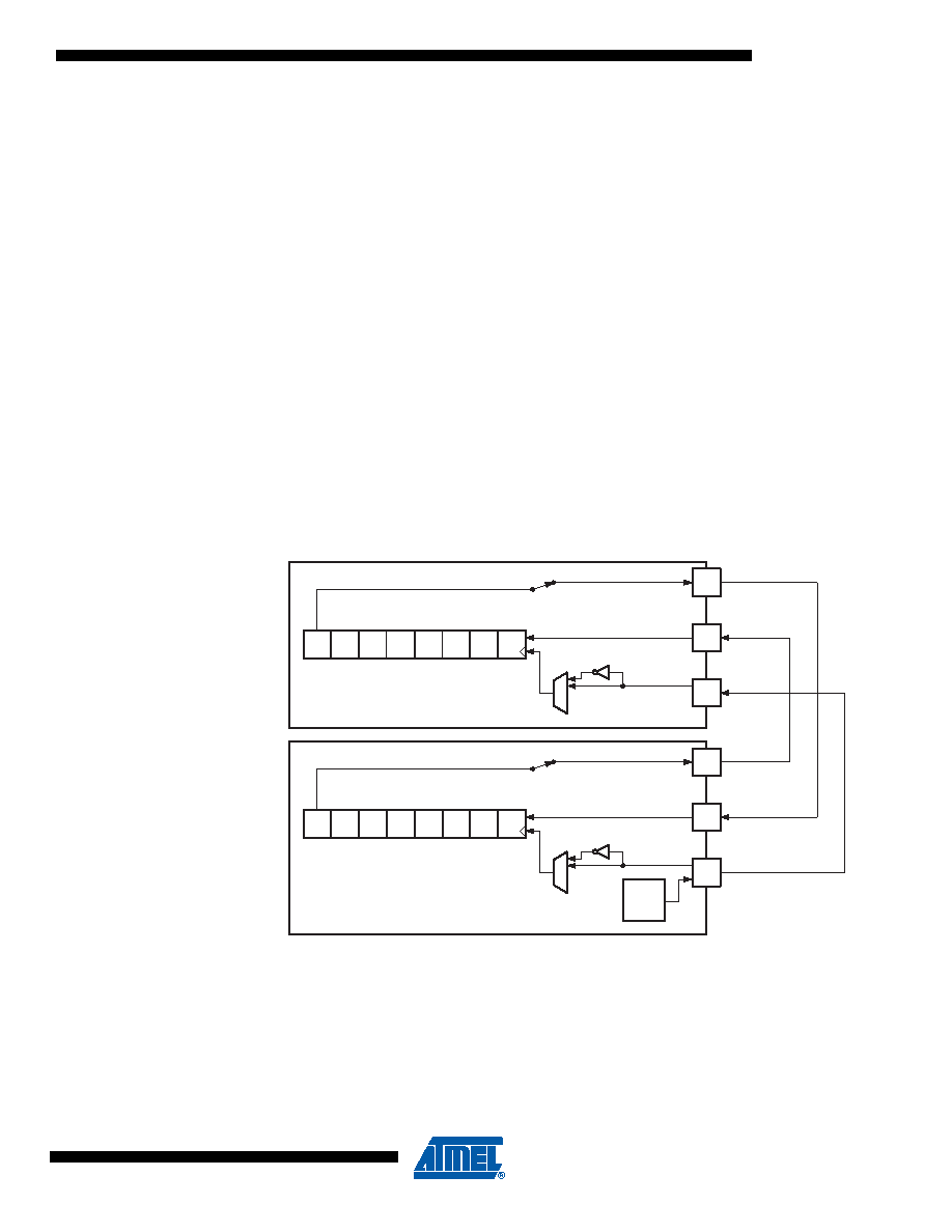
Figure 14-2. Three-wire Mode Operation, Simplified Diagram
Figure 14-2 shows two USI units operating in three-wire mode, one as Master and one as Slave.
The two USI Data Registers are interconnected in such way that after eight USCK clocks, the
data in each register has been interchanged. The same clock also increments the USI’s 4-bit
counter. The Counter Overflow (interrupt) Flag, or USIOIF, can therefore be used to determine
when a transfer is completed. The clock is generated by the Master device software by toggling
the USCK pin via the PORTA register or by writing a one to bit USITC bit in USICR.
SLAVE
MASTER
Bit7
Bit6
Bit5
Bit4
Bit3
Bit2
Bit1
Bit0
DO
DI
USCK
Bit7
Bit6
Bit5
Bit4
Bit3
Bit2
Bit1
Bit0
DO
DI
USCK
PORTxn
发布紧急采购,3分钟左右您将得到回复。
相关PDF资料
PIC16F727-E/P
IC PIC MCU FLASH 8KX14 40-DIP
PIC16F871T-E/PT
IC MCU CMOS 20MHZ 2K FLSH 44TQFP
PIC16F871T-E/L
IC MCU CMOS 20MHZ 2K FLSH 44PLCC
PIC16F871-E/PT
IC MCU CMOS 20MHZ 2K FLSH 44TQFP
PIC16F871-E/L
IC MCU CMOS 20MHZ 2K FLSH 44PLCC
PIC16F870T-E/SS
IC MCU CMOS 20MHZ 2K FLSH 28SSOP
PIC16F870T-E/SO
IC MCU CMOS 20MHZ 2K FLSH 28SOIC
PIC16F84AT-20E/SS
IC MCU CMOS 20MHZ 1K FLSH 20SSOP
相关代理商/技术参数
PIC16F872T-E/SS
功能描述:8位微控制器 -MCU 3.5KB 128 RAM 22 I/O RoHS:否 制造商:Silicon Labs 核心:8051 处理器系列:C8051F39x 数据总线宽度:8 bit 最大时钟频率:50 MHz 程序存储器大小:16 KB 数据 RAM 大小:1 KB 片上 ADC:Yes 工作电源电压:1.8 V to 3.6 V 工作温度范围:- 40 C to + 105 C 封装 / 箱体:QFN-20 安装风格:SMD/SMT
PIC16F872T-I/SO
功能描述:8位微控制器 -MCU 3.5KB 128 RAM 22 I/O RoHS:否 制造商:Silicon Labs 核心:8051 处理器系列:C8051F39x 数据总线宽度:8 bit 最大时钟频率:50 MHz 程序存储器大小:16 KB 数据 RAM 大小:1 KB 片上 ADC:Yes 工作电源电压:1.8 V to 3.6 V 工作温度范围:- 40 C to + 105 C 封装 / 箱体:QFN-20 安装风格:SMD/SMT
PIC16F872T-I/SS
功能描述:8位微控制器 -MCU 3.5KB 128 RAM 22 I/O RoHS:否 制造商:Silicon Labs 核心:8051 处理器系列:C8051F39x 数据总线宽度:8 bit 最大时钟频率:50 MHz 程序存储器大小:16 KB 数据 RAM 大小:1 KB 片上 ADC:Yes 工作电源电压:1.8 V to 3.6 V 工作温度范围:- 40 C to + 105 C 封装 / 箱体:QFN-20 安装风格:SMD/SMT
PIC16F872T-I/SS033
制造商:Microchip Technology Inc 功能描述:
PIC16F873-04/SO
功能描述:8位微控制器 -MCU 7KB 192 RAM 22 I/O RoHS:否 制造商:Silicon Labs 核心:8051 处理器系列:C8051F39x 数据总线宽度:8 bit 最大时钟频率:50 MHz 程序存储器大小:16 KB 数据 RAM 大小:1 KB 片上 ADC:Yes 工作电源电压:1.8 V to 3.6 V 工作温度范围:- 40 C to + 105 C 封装 / 箱体:QFN-20 安装风格:SMD/SMT
PIC16F873-04/SO
制造商:Microchip Technology Inc 功能描述:8BIT FLASH MCU SMD 16F873 SOIC28
PIC16F873-04/SP
功能描述:8位微控制器 -MCU 7KB 192 RAM 22 I/O RoHS:否 制造商:Silicon Labs 核心:8051 处理器系列:C8051F39x 数据总线宽度:8 bit 最大时钟频率:50 MHz 程序存储器大小:16 KB 数据 RAM 大小:1 KB 片上 ADC:Yes 工作电源电压:1.8 V to 3.6 V 工作温度范围:- 40 C to + 105 C 封装 / 箱体:QFN-20 安装风格:SMD/SMT
PIC16F873-04/SP
制造商:Microchip Technology Inc 功能描述:IC 8BIT FLASH MCU 16F873 SDIL28